

Discover more from Fabricated Knowledge
I want to start with other segments of Semicap but it’s pretty much impossible to do without starting with the foundational Lithography step. For many generalists, Lithography is the one step in semiconductor manufacturing that makes the most sense and is the easiest to grasp, or at least grasp its relative positioning within the manufacturing value chain. The valuation multiple reflects that. But despite the hype – Lithography is the real deal and very important to understand before we go any further.
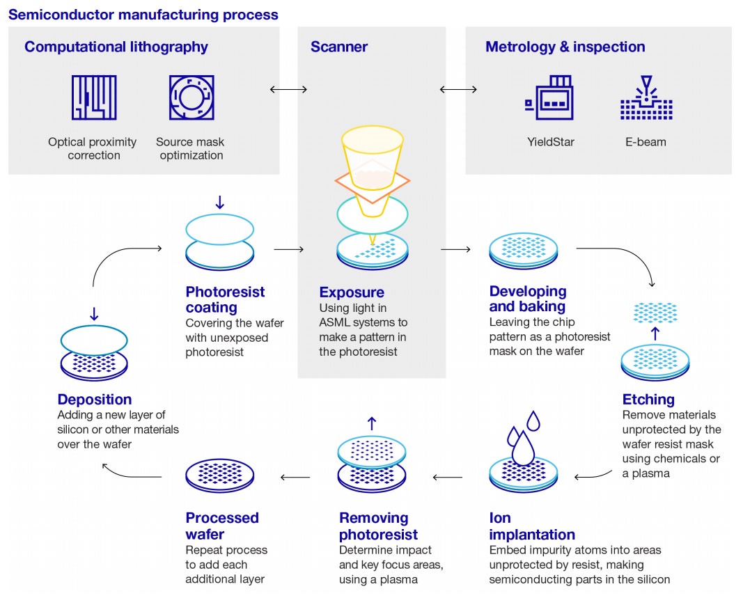
How Semiconductors are Made
(This is a partially expanded version of the basic introduction I wrote - with emphasis on photoresist coating, exposure, developing, and baking)
The original definition of Lithography is “the process of printing from a plane surface (such as a smooth stone or metal plate) on which the image to be printed is ink-receptive and the blank area ink-repellent”. What is so wonderful is that despite the huge differences in complexity for semiconductors, this is essentially correct for lithography but instead of using a stone, we are using light to produce patterns on a piece of purified sand.
Instead of ink like old lithography, today we use photoresist or a light-sensitive polymer that changes its composition when the photoresist interacts with light. We cannot overstep the importance of Lithography, as it is at the heart of the modern semiconductor era. When I read the history of Fairchild Semiconductor, one of the things that caught my eye was a very brief mention of Lithography.
“In contrast, Fairchild Semiconductor researchers selected what they viewed as the best most promising techniques for the long run…. Among these approaches were baron and phosphorus diffusion, oxide masking, photolithography, and aluminum evaporation.”
One of Fairchild’s many critical inventions was photolithography which leads to modern manufacturing. Before photolithography, transistors were “grown” as silicon crystals– similar to how wafers are formed. But photolithography was the “eureka” moment that helped push transistors from being handmade and artisanal to standardized and mass-produced. Photolithography allowed for semiconductors to walk down the path it is on today, enabling Moore’s law and the dramatic geometry shrink.
Photolithography in this regard deserves all the hype it gets. The core goal of making a semiconductor is to deposit film, pattern the semiconductor, or dope it. But for this to happen - you must use Lithography. Lithography is like the prep work for all the following steps. You can’t consistently make any other step without sketching it out in lithography first. Let’s walk into a very granular step by step of the lithography portion of this diagram.
So Photolithography doesn’t start at just the exposure part of the story – the photoresist coating of the wafer is the pre-step that helps exposure be successful. In fact, something I want to highlight when I talk about Semi cap is every single step has pre-steps and post steps, and each process works deeply together. It takes a village to build a semiconductor. For lithography, in particular, these steps are the coating, pre, and post bake process.
Cleaning and Photoresist Coating
Before you can expose a wafer to light, you must coat the wafer in a photoresist film. To do so you have to first clean the wafer, and then “pre-bake” the wafer to remove the water. The wafer is cleaned with ultrapure water, heated to 200-400C for 60 minutes to evaporate, and then is allowed to cool. After the pre-bake, the surface of the wafer is usually coated with SiOH – which is bonded to the surface. This removed via chemical means which can act as a primer for the coating the photoresist. Afterward, we apply the photoresist layer.
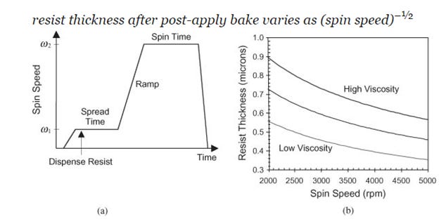
A uniform layer of perfectly even photoresist is added to the wafer, and the way that is achieved is spin coating. The resist is made into a liquid (or sometimes a gas), and then sprayed onto the wafer, and then spun at high speed. The centrifugal force flings the resist to the edge of the wafer and coats it in a uniform layer. Every type of photoresist (there are of course different types!) has different optimal rotation levels, and that has to be figured out by engineers onsite. The right process is often found experimentally.
Source: Fundamental Principles of Optical Lithography: The Science of Microfabrication
With the resist flung to the edges of the wafer via centrifugal forces, a thin film now coats the wafer. The actual spin rotation for a wafer is found out experimentally as well and depends on the desired resist thickness. Spin forces max out at up to 2000 rpm, and the result is a thin layer applied with an edge bead from the surface tension at the edge of the wafer.
Source: https://www.intechopen.com/books/updates-in-advanced-lithography/resist-homogeneity
This edge cannot be allowed, but physically removing it will cause participles in the chamber, so a stream of chemicals remove this specific edge while the wafer spins. Now comes baking the wafer.
Post-Apply Bake
At this point, your wafer is covered in photoresist liquid, but you’re going to want it to be a bit thinner than that. There still is a decent amount of solvent in the resist, and you have to bake that away. Also when the resist is heated, adhesion and the actual property of the resist is changed. It’s kind of a delicate process, and above 70C the resist will decompose, so instead of baking it in an oven (like the 1980s), the preferred method is called a hotplate. You move a superheated high-mass metal plate close to the silicon for 20 seconds and it will “bake” the resist into its final form. You usually have a chill plate afterward to set the bake, and then you’re finally ready for the actual lithography. All of these steps happen before the wafer is put into a lithography tool.
Alignment and Exposure
At this point, we have a thin film that is resistant to most chemical solutions but is not resistant to light. When we expose the photoresist to light, it gets converted to carboxylic acid, which can be removed with a base solution. We finally can “pattern” something on the silicon wafer. There are many ways that lithography can happen, namely contact (mask on the wafer), proximity (mask near wafer), and projection (mask away from the wafer). The most popular today is the projection method (EUV) and sometimes immersion (mask away from wafer but water as a film between the lense and wafer).
There are two ways that the wafer can be exposed to light, scanning, and stepping. In modern times we use step AND scan. Scanner exposes a smaller portion of the wafer and does it slowly across the entire wafer. While a stepper’s mask focuses on a single part of the wafer and then repeats that step to nearby parts of the wafer.
Source: Fundamental Principles of Optical Lithography: The Science of Microfabrication
Today we use Step and Scan, or a hybrid approach of the two.
Source: https://slideplayer.com/slide/9416386/
Step and Scan is kind of the best of both worlds hybrid solutions. Scanners are much more efficient because of a smaller output of light, while step and scan use the higher efficiency of the scanner process while simplifying it with the step process.
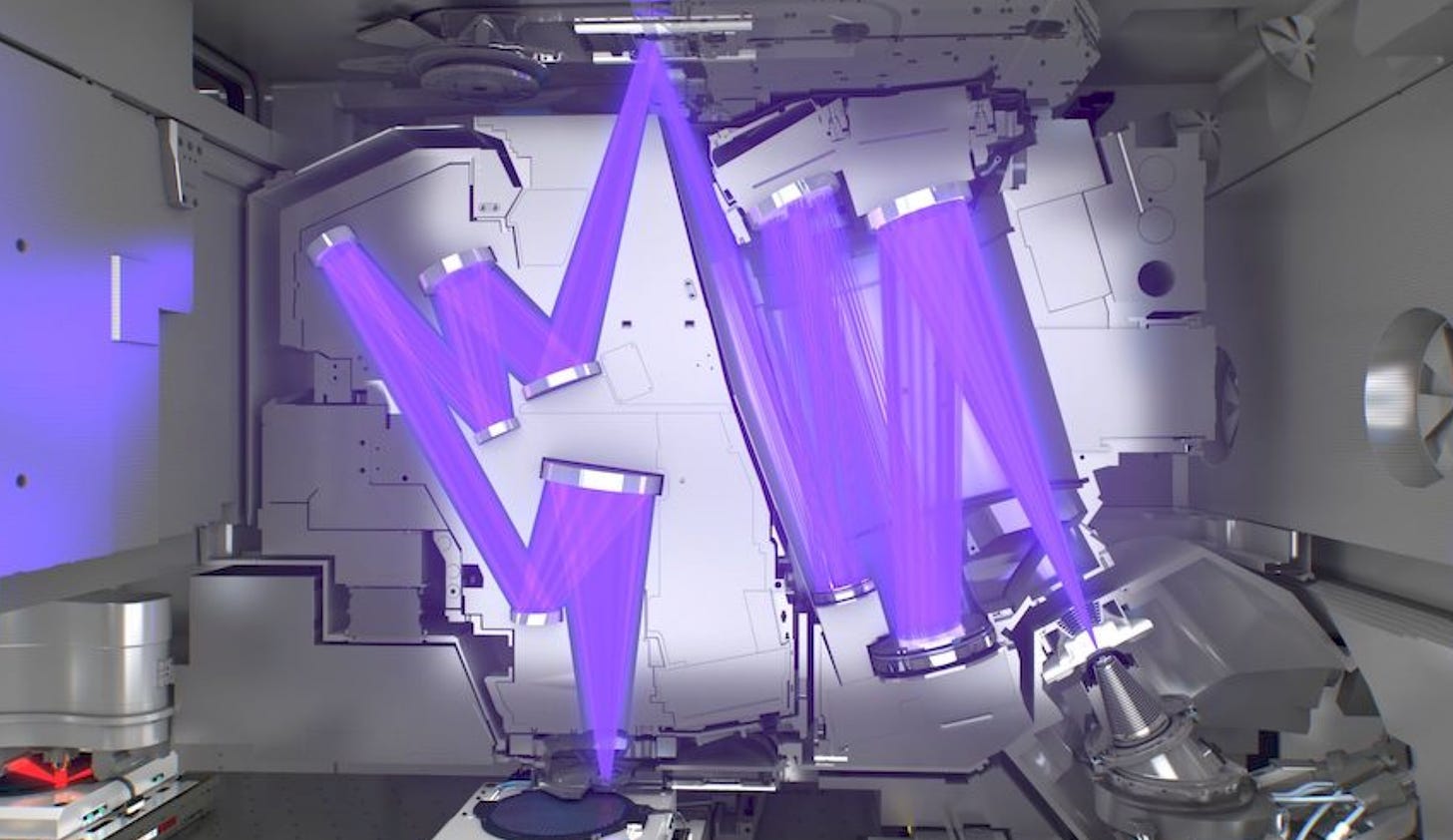
But even getting that beam of light to the wafer is really complicated. This is not like just flashing a laser through a mask onto the wafer – it’s more like flashing a super finicky light source that wants to bounce and reflect everywhere and perfectly hitting the wafer so there is no distortion, phase shift, or polarization. This is no easy trick.
The beam is split into smaller parts, aligned so that the EUV beam hits the wafer at the perfect angle, and not create any distortion. Reminder if it was to hit the wafer at a wrong angle, your entire transistor would be ruined! It is aligned to the tiniest detail and has to hit the mask at a specific angle and precision as well. Calibrating this is a miracle.
And this is just the tip of the iceberg. There are practical engineering problems with lights tilt, polarization, light flares, the reflection angle is correct, and many many more. All of these problems were present at high-NA (the primer is written with a high-NA mindset first) but today at EUV (Extreme Ultraviolet) this problem is much harder and even more precise. This is the pure technology and trade secret advantage that ASML has over everyone. They are the first and only company to ever bring it to market and engineer the solution to the advanced physics problem of shooting a beam of light accurately onto a silicon wafer.
The light beam hits the mask, and prints a pattern on the wafer. The photoresist that remains is a kind of relief – and the pattern achieved is like carving into marble to create your desired outcome.
Developing and Baking
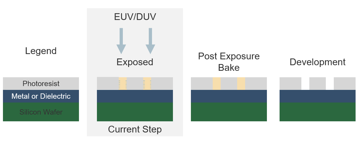
But of course – we are not done yet! When the actual process is done, there are still problems with resist ridges. When the light strikes the wafer, the substrate usually reflects some light creating slight inconsistencies and creating ridges in the walls.
Source: Fundamental Principles of Optical Lithography: The Science of Microfabrication
This is corrected by post-exposure bake – where the waves are smoothed out using temperature. But remember that it can’t be too hot or the photoresist melts altogether. This is once again a process best found by experimenting. This context helps explain why certain fabs are “better” than others. Practical experience of using the tools and solving the day-to-day problems of lithography and manufacturing is a learning curve that only 3 global fabs really do for leading-edge nodes.
Development is the last step, and this is where the photo (think of a film photo) is developed. Applying a developer to the photoresist now results in an interesting process, the places that the light has been exposed to light now have been removed, and there is a pattern in its place. We now move to the final post bake session – where we harden the resist so it can resist etching or other processes. (We will discuss etch + other steps later).
Metrology
There’s been a lot of steps and work done, but it’s time to measure and inspect what you’ve done so far. Between each step, the wafer inspects to see if particles messed up the process, or wafers with problems that are fixable can be sent back to the beginning of the process and reworked. If it can’t be reworked – they will be scrapped – oftentimes because the complexity of reworking outweighs trying to fix a wafer.
For today – we are going to leave semiconductor manufacturing here. This is all to set up the relief for other processes in semiconductor development, and we will discuss this in further primers.
I hope this in-depth explainer helps – but more importantly I hope you get a few important takeaways.
1) There are many steps in Semicap and they are all interrelated.
2) Each step has an important role to play, and you must try the steps to figure out if your fabrication is working or broken. This creates cumulative IP and learning of the tools.
3) Solving these problems are really hard, and the companies that consistently bring good tools to market that work has a kind of deep trade-secret level IP. It is one thing to make a EUV beam, it’s another to form it and make it consistently hit a wafer at the right angle to make a mask pattern. The engineering of the latter is why these companies are valuable.
Where We are Today
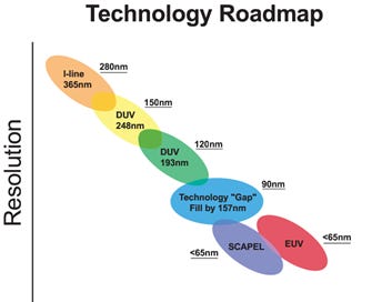
I just described the process as laid out via a textbook that discusses the high-NA process that was standard in the 2010s. Where we are today is something called EUV. EUV is the evolution of the smallest wave of light we currently can manipulate and is the cutting edge of lithography technology.
EUV stands for “extreme ultraviolet“ lithography – and is the next generation of light used to manufacture semiconductors, standing at ~13.5nm compared to previous ~193nm wavelengths of light. EUV is an engineering marvel that is best explained by watching - this is a wonderful youtube video to visualize what is happening.
EUV is created by blasting a piece of molten tin with a laser and then manipulating the light source to be smaller and eventually hitting the substrate. The core problem of EUV is making the light source (it’s extremely temperamental and precise), and then harnessing EUV, which is much weaker and not as constant as a direct laser source. ASML of course has finally figured out how to master this technology.
The Business of Lithography
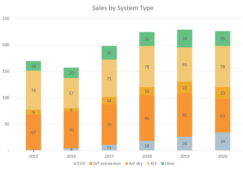
I have pretty much exclusively talked about science so far – and it’s time to talk about the actual business of Lithography. ASML is the company I will primarily be focusing on – as it is unlikely that Nikon will ever develop EUV, and its revenue is essentially flat over a long period of time. For a very brief overview of the runner up company, refer to the total system sales of Nikon historically.
Nikon interestingly is a huge Intel partner, but that’s an aside. Nikon today sells i-Line systems, KrF, ArF, and ArF Immersion. Nikon’s best days (as a semiconductor company) are likely behind them. Some more history about their historical leadership (their first machine was in 1976!) is available here.
Anyways – onto ASML. ASML is the dominant business here, and to talk about Lithography in modern times is pretty much to talk about ASML.
ASML - The History Before the Monopoly
ASML is pretty unique in that it was a European company founded during the American semiconductor revolution. Founded in 1984 as a joint investment from Philips and Advanced Semiconductor Materials International, ASM Lithography was founded in the Netherlands and launched its first product, the PAS 2000 stepper (refer to above for Step lithography). ASML also in 1986 established their JV with Carl Zeiss, which of course is one of the reasons for their leadership today.
The 1980s was the era of IBM personal computers, the first decade of the microprocessor, and likely the zenith of American global semiconductor leadership. Innovation was almost a monthly cadence, and ASML at the time was a tiny fish in a huge pond. At the time, ASML was a relatively niche supplier, and the Japanese lithography systems and companies were battling it out against the Americans. ASML was kind of a nobody, struggling to find relevance and customers.
ASMI (ASM:NA) actually even pulled out of the JV, and ASML had to reach out to Phillips for a lifeline. But ASML would pull through and introduce the PAS 5500 lithography platform. What’s interesting is despite its age - 90% of the PAS systems ever sold are still in use today. Nothing ever really goes to waste in semicap, just refurbished and reused. PAS made ASML a viable and strong competitor, but not exactly the de facto leader.
The real step change was the TWINSCAN system and the measuring and exposure, which helped improve throughput meaningfully. Additionally, in 2003, TWINSCAN XT:1700i was the first volume immersion Lithography system aka the last platform of Lithography before EUV. Even today on trailing nodes, Immersion Lithography is the workhorse system for everything ex-EUV in semis. This is the product that took them from strong contenders to absolute leaders. While this video is not a product overview, you can see an example of what Immersion lithography looks like here, and an example of TWINSCAN here.
Twinscan narrowed the competition to two companies (ASML and Nikon), but with ASML with a stronger roadmap towards EUV. I think for those wondering about the competition at the time, this is a great article to refer to that kind of compares the two immersion systems head to head. Interestingly, even though it is 2006, EUV of course is mentioned and top of mind. The path forward has always been EUV and the industry knows this. It has been talked about and anticipated for so long, and despite delays, we are finally here. And that brings us to the last stage of ASML’s life, the EUV Monopoly.
ASML and the EUV Era
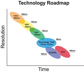
ASML has been working on EUV for a long time. I think this slide helps put it into context. EUV as a concept was pretty well understood on how it would happen in the 1990s, but making it a reality was an engineering nightmare. This has been a work in progress for 15+ years - and ASML has a great timeline from their investor materials below.
Beyond just the actual engineering, EUV was a ~10s of billion dollars investment. Getting it to market was pretty hard, and it is unlikely another company will do it for a considerable time. ASML had a very unique program called the customer co-investment program and took investments from Intel, Taiwan Semiconductor, and Samsung in a large share offering to help get the necessary capital to finish EUV into the product. But regardless I don’t really think the engineering focus is really important on how they did it, I think it’s just nice to point out the long road it took to get here. ASML now is the only EUV Lithography maker in the world and will sell 100% of systems for products that use EUV (5nm and below). Additionally, an entrant would be flagged for 5-10 years before they could ever enter this market.
Paired with the assumption that the vast majority of systems will be EUV in 2025 and onwards, you can kind of get the market’s excitement for ASML. As long as Lithography is an important part of wafer fab equipment (WFE), ASML will have a stable market share that should persist and grow. So from that perspective, ASML is a monopoly that the world cannot make go away because then we would take the forward progress of semiconductors out of our future. Even if we were to opensource the technology, it is not exactly the science but the engineering that is a huge problem to make the equipment as well.
I think what’s more staggering and hard for ASML has not been the actual EUV, but the process of even shipping the tool to customers. Each EUV tool costs ~300m+ EUR to make, and has to be made in a special clean room the size of a large fab itself. The actual machines themselves weigh so much they will break the foundations of typical buildings, and the process of getting it to a plane to be shipped is another custom made process. The machine is so large it has to be broken into 6 parts to be shipped, and the cleanroom it is made in has to be a specific temperature the entire time because even a temperature difference will mess with the machine’s calibration.
All of these were problems that were solved to make EUV possible, and I don’t think that is easily replicable even with IP or patents. It’s not just a tool, it’s a custom supply chain to even build and move the tool. ASML is truly irreplaceable and likely unreplicable. It could be done again, but the trade secrets and learnings to get the tool to work would likely be billions of dollars again, and an investment that even a nation (I’m thinking of China) probably couldn’t pull off. This is why there is such a high premium on the company, it truly is a once in human history kind of achievement so far.
What That Means for ASML the Stock
Historically Lithography has been approximately ~20-30% of total WFE, and so ASML should get somewhere in that neighborhood of revenue as an annuity forever. WFE grows usually at a ~7% CAGR over long periods of time, and EUV currently is taking a relative share of spend in WFE as fabs upgrade to EUV. So I would say ASML has the ability to grow 15-20% for 5-10 years with a terminal value of ~5-7% growth until we figure out another way to make chips.
Currently, their actual results for the last 5 years are in-line with the guess, growing at a 15% revenue CAGR from 2014-2019, and a bit higher for 2020 (16% trailing). That makes sense to me as the ASML revenue ramp just kind of started. The important distinction here though is that there are two line items of revenue at ASML, system sales, and installed base management.
Currently, net system sales are growing much much faster than installed base management, but eventually, as the new systems have to be maintained the installed base management will start to grow faster. Right now they are selling new machines but many of them are not even in production currently and are being qualified and assembled. As they start to actually run wafers, the service and spare business will start to pick up as well. Additionally, the service business has the benefit of being subscription-like in nature and considering that 90% of their machines are still in service, the business of maintaining and repairing their systems is likely a 20+ year annuity. So this portion of the business should grow double-digit to match their total installed base.
Gross Margins
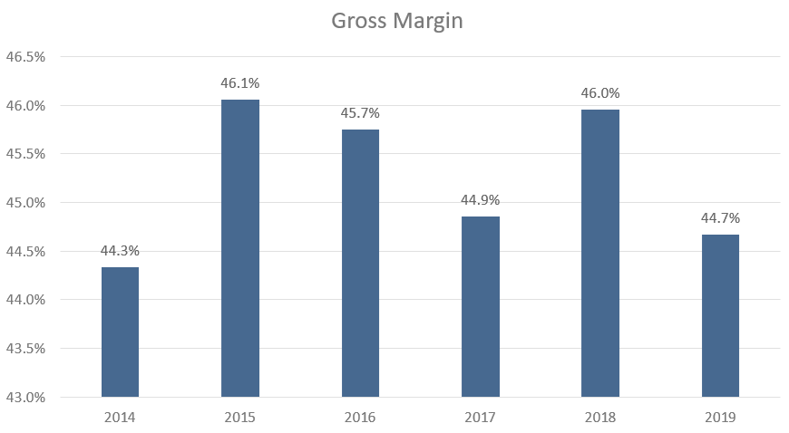
There is a little bit of nuance here - because while the revenue has been growing, gross profit is a bit more complicated. As ASML has been ramping EUV revenue, it’s been extremely dilutive to gross margins.
Currently, EUV is meaningfully below corporate average, with early ramping at 20% gross margins, and current service margins are just at breakeven. Over time this should improve as the supply chain matures, and ASML believes that eventually, it will exceed DUV-like margins at over 50%+ over time. So as EUV reaches maturity and eventually scales to 50-60 systems annually, the gross margin should meaningfully improve. But that may take some time.
This is where modelers could go nuts. Estimate revenue by system type, by gross margin, etc. But honestly, the easier way to think about ASML is just to follow their long term revenue target. They put it out in 2016, and then again in 2018, and it’s been reasonably accurate since. No one really knows the exact cadence the systems will be ordered, but EUV is inevitable. The scenario is going to end up between the moderate and high scenarios, and their 2016 estimate for 20202 was pretty accurate.
Their moderate-upside 2020 model was between $12.9-14.7 in 2020, as compared to ~13.3 billion as consensus. I believe that the best way is just to make a simple DCF of 2025 between moderate and aggressive, and you find a range of values for what ASML should trade at. I use ~21000 compared to their range of 19.4 - 24.3 billion in guidance.
Let’s put that into a DCF for you really quickly. I just did 100% NI/CFO for simplicity's sake - as they are likely close to the maximum of working capital improvements.
This is one of my favorite DCF’s to do (don’t kill me on accuracy here - it’s illustrative) because it can be either viewed as cheap or expensive. If I really use a 4% terminal value for growth, it’s cheap. If I use a hefty 35x exit multiple, it’s very expensive. Note the 7% discount rate - but I think this still gets you to the crux of the argument. If you view this as a permanent asset (I do) it can be cheap from time to time. But you can’t make it work on a long term DCF with an exit rate. Even a 35x exit rate at a 7% discount gets you to “overvalued”. But clearly, the long rate of growth is going to be pretty impressive if the management team put out a long-term target this ambitious.
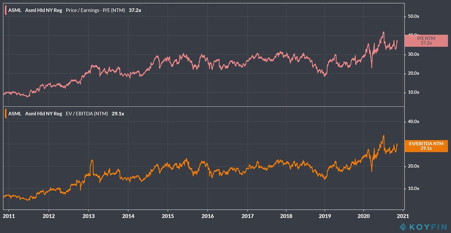
In my eyes - there are times when it becomes “cheap” and worth a buy. During March it briefly was sub 25x earnings, and that always seems to be an alright price for ASML. It’s touching 40x right now - and the risk-reward there just makes it so much harder to feel super confident. It’s clearly priced as a long term bond, with a 1-2% FCF yield and a double-digit FCF growth rate. If rates move - well of course that multiple should get crushed.
But in terms of “will ASML be around in 10 years” I think the write-up above about the technology and particularly defensive position ASML has makes it clear that they are a forever asset. But you are going to have to wait a long time to own it at a good price.
From time to time (2019 is particularly glaring) there are cycles that make this company cheaper than historical - and that is always an opportunity. Right now the ramp to EUV is appreciated in the market and the company is expensive. But obviously, it isn’t the only semicap company in the world. Just the first one you should understand before we go deeper into semicap.
I think next time we will talk about etch!
Glossary and Other Notes
What is Immersion Lithography – you can coat the lens with ultrapure degassed water with a new refractive index as the immersion liquid – and this small puddle of water between the light source and wafer has to be constantly filtered to reduce impurities. The refraction of water helps keep the angle of light to hit the resist the same, and thus helping extend control of the light to the wafer. The challenges for making this into mass production cannot be overstated. You must constantly filter water over the wafer while the high-speed lithography occurs on the wafer.
This might sound familiar, but Immersion Lithography was what was being used before EUV. ArF Immersion in particular, and there was an extremely high profile litigation issue where eventually Zeiss, ASML, and Nikon settled.
What is E-Beam? – E-Beam is primarily a wafer inspection tool. Whenever they make the optical cuts into the wafer, they have to inspect errors right? Well at EUV we are struggling to use lithography, and so e-beam inspection is starting to be used. E-beam has meaningful problems with throughput, but optical just isn’t cutting it for advanced nodes anymore. Especially advanced 3D architectures, optical inspection is just not going to hold up. ASML bought Hermes Microvision to launch into E-beam. AMAT / KLAC also have products here to address this need. While this is not a primary business for ASML, it is tangential to what they offer.
Who makes Photomasks? - Here is a list of meaningful vendors. Everyone has a small or partial business here, but I believe Lasertec is consistently a standout supplier. Making the actual mask is each fab’s secret sauce and extremely secretive. This is trade secrets folks!
Who makes the Developer / Coater - Tokyo Electron - this slide is a really great overview of their position immediately before and after lithography.
This is a market that Tokyo Electron has completely got on lock. 91% share is about as much of a monopoly as ASML has on Lithography.
Subscribe to Fabricated Knowledge
Let's learn more about the world's most important manufactured product. Meaningful insight, timely analysis, and an occasional investment idea.

















Thanks for the write-up! It's very interesting to peel back the layers on how semis are made. Correct me where I am wrong. The process you described is making one layer of the wafer. Do the # layers increase as nodes get smaller or that is not correlated? Would EUV be used in making all those layers or only the smallest patterns?
Thanks for write-up, super helpful as always- may I ask, i get it’s purely illustrative but is there are a reason you’re using net income (so net of d&a) and still subtracting capex in your DCF?
Also referring to your previous posts - if they own 100% of the best incremental technology and we think demand for semis will grow exponentially (due to AI) I would have thought the CAGR implied by the 2025 target is not particularly impressive? Or I am missing something in the bargaining power they have with customers or how the demand for their product correlates with semis demand?
Many thanks